Definition of Combinational Logic:
Combinational logic is a type of digital circuit where the output depends only on the present input values, not on any past inputs or previous output states. It performs operations like addition, subtraction, comparison, and data routing using logic gates such as AND, OR, NOT, NAND, NOR, XOR, and XNOR. It does not use memory or feedback, so it has no storage elements.
The block diagram of a combinational logic circuit is shown in the diagram below.

Classification of Combinational Circuits
Combinational circuits can be classified as:
i) Code Converters
ii) Adders
iii) Subtractors
iv) Comparators
Adders:
The addition of two binary digits is the most basic operation performed by digital computers.
Classification of Binary Adders:
i) Half Adder
ii) Full Adder
Half Adder:
A half adder is a combinational logic circuit with two inputs and two outputs. It is the basic building block for adding two single-bit binary numbers. This circuit produces two outputs: carry and sum. The half adder is the logic circuit that adds the two bits and generates the sum bit (S) and carry bit (C) as outputs. The functional block diagram and truth table of a half adder are shown below.


For sum : S = A’ B + A B’ = (A ⊕ B)
For Carry : C= AB
The logic diagram of the implementation of the Half Adder circuit is shown below.
Limitations of a half adder:
Here are the drawbacks of the half adder.
- It cannot add the carry from a previous addition.
- It can only add two 1-bit numbers, not larger numbers.
- You need extra circuits to add multi-bit numbers.
- To do complex addition, many half adders and other parts are needed.
- Because of its limits, it is not used alone in real digital systems.
Full Adder:
A full adder is a combinational logic circuit that adds three single-bit binary numbers: two significant bits and a carry input from a previous stage. It has three inputs (A, B, and Carry-in) and two outputs: Sum and Carry-out.The general block diagram and truth table of the full adder are shown below.


The Boolean expressions for sum and carry are:
 .
.
The logic diagram implementation of the Full Adder circuit is shown below.

Subtractor:
A subtractor is a combinational logic circuit that performs the subtraction of two binary numbers. There are two types of subtractors:
1. Half Subtractor:
2. Full Subtractor:
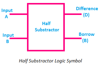
Half Subtractor:
A half subtractor is a simple combinational logic circuit that subtracts one single-bit binary number from another and gives two outputs: the difference and the borrow. In simple words, A half subtractor finds the difference between two bits and tells if borrowing is needed for the next subtraction.The Block diagram and truth table of a half subtractor are shown below.
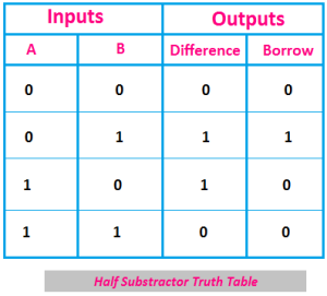
Based on the above truth table, the Boolean expressions for the half subtractor are:
Difference (D) = A’B+AB’=(A ⊕ B)
Borrow (B) = A’ B
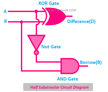
The logic diagram of the implementation of a half subtractor is shown below.
Drawbacks or Limitations of Half Subtractor:
Here are the Major drawbacks of the half subtractor:
- It cannot take a borrow from the previous stage.
- It can only subtract two single-bit binary numbers.
- It cannot be used directly for multi-bit subtraction.
- Extra circuits are needed for subtracting larger binary numbers.
- It is not suitable for complex or real-world digital systems.
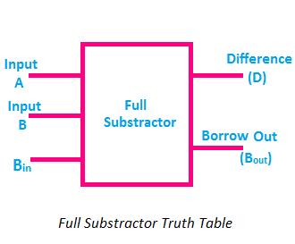
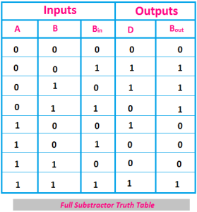
Full Subtractor:
A full subtractor is a combinational logic circuit that performs the subtraction of three binary bits by taking into account a borrow from the previous stage. It has three inputs: A, B, and Bin. The Functional block diagram and truth table are shown below.
The logic diagram implementation of the Full Subtractor is shown below.
Why full subtractor more reliable than a half subtractor?
A full subtractor is more reliable than a half subtractor because it can handle the subtraction of binary numbers that require borrowing from a previous stage.
- A half subtractor can only subtract two single bits and cannot consider a previous borrow.
- A full subtractor can subtract two bits and take into account a borrow from a previous calculation, making it suitable for multi-bit binary subtraction.
- So, for real-world binary subtraction in computers and digital systems, the full subtractor is more reliable and practical than the half subtractor.
Applications of Subtractor:
- Binary Subtraction: Subtractors are used in digital circuits to perform binary subtraction in computers and calculators.
- Arithmetic Logic Unit (ALU): Subtractors are a key part of the ALU in microprocessors and microcontrollers for performing arithmetic operations.
- Digital Counters: Subtractors help in designing up-down counters where counting backward is needed.
- Comparators: Subtractors are used in magnitude comparators to find the difference between two binary numbers.
- Signal Processing: In digital signal processing (DSP), subtractors help in filtering and modifying signals.
- Subtractors are widely used wherever we need to find the difference between numbers in digital electronics.
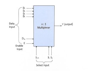
Multiplexer (MUX):
A multiplexer(mux) is a combinational logic circuit that has several or many inputs and only one output. A multiplexer contains 2n input lines, n selection lines, and gives a single line output. The selection of the input determines that the input should be connected to the production.
The General function block diagram of a mux is shown below.
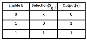
2:1 Multiplexer :
A 2:1 multiplexer has two data inputs, D0 and D1, one select input S, an enable input E, and one output Y. The block diagram of a 2:1 multiplexer is shown in the diagram
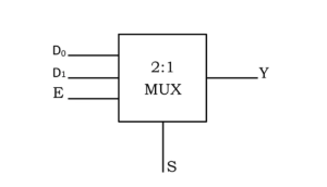
The Boolean expression of a 2X1 MUX is:
y =ES’D0 +ESD1
Y =E(S’D0 +SD1)
4×1 Multiplexer
A 4×1 multiplexer (MUX) is a combinational logic circuit that selects one input from four different input signals and forwards it to a single output line. The selection of the input is controlled by two selection lines (S0 and S1).The block diagram and truth table of a 4×1 mux are shown below the diagram.
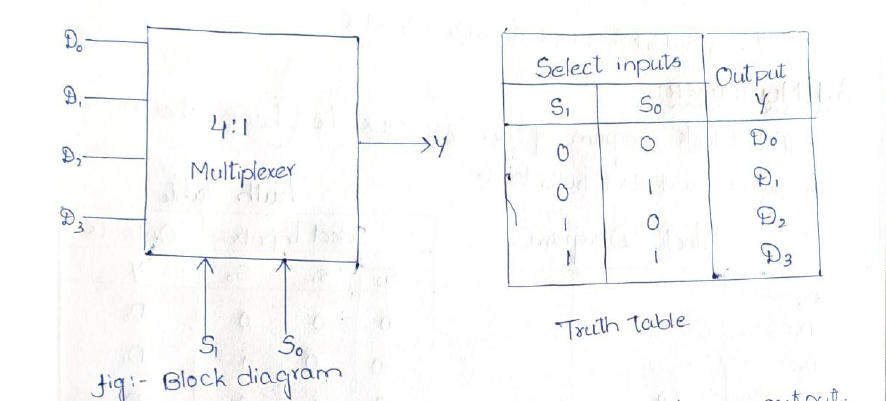
The boolean expression of 4 xa mux is:
Y=S’1S’0D0+S’1S0D1+S1S’0D2+S1S0D3
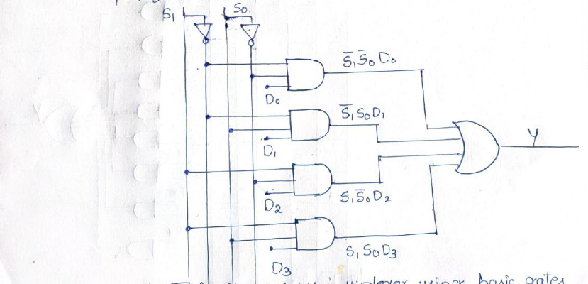
The logic diagram implementation of 4×1 mux is
8×1 Multiplexer (MUX)
An 8×1 Multiplexer (8×1 MUX) is a digital combinational circuit that selects one input line from eight different input lines and forwards it to the single output line, based on the combination of three selection (control) inputs
The functional block, and truth table are shown below diagram.
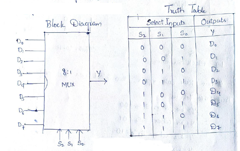
Boolean expression of 8×1 mux is:
Y=(S2′S1′S0′)D0+(S2′S1′S0)D1+(S2′S1S0′)D2+(S2′S1S0)D3+(S2S1′S0′)D4+(S2S1′S0)D5+(S2S1S0′)D6+(S2S1S0)D7
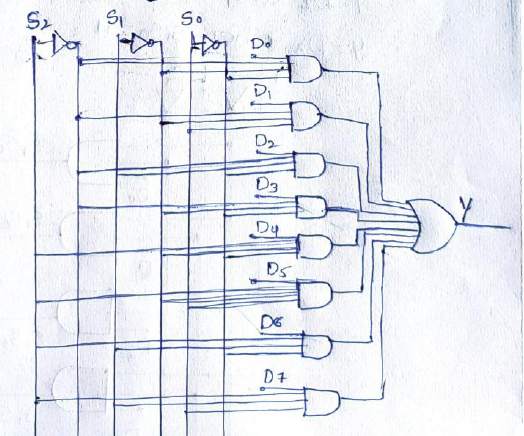
logic diagram implementations of 8×1 Mux can be drawn as
Applications of a Multiplexer:
The applications of the multiplexer are listed below
- It is used as a data selector to select one out of many data inputs.
- It is used for the simplification of logic design.
- In the data acquisition system.
- In designing the combinational circuits.
- In the D/A converters.
- To minimize the number of connections.
Demultiplexer (Demux)
A demultiplexer (demux) is a digital electronic device that takes a single input signal and routes it to one of many output lines, based on control or select signals. It essentially performs the reverse operation of a multiplexer.
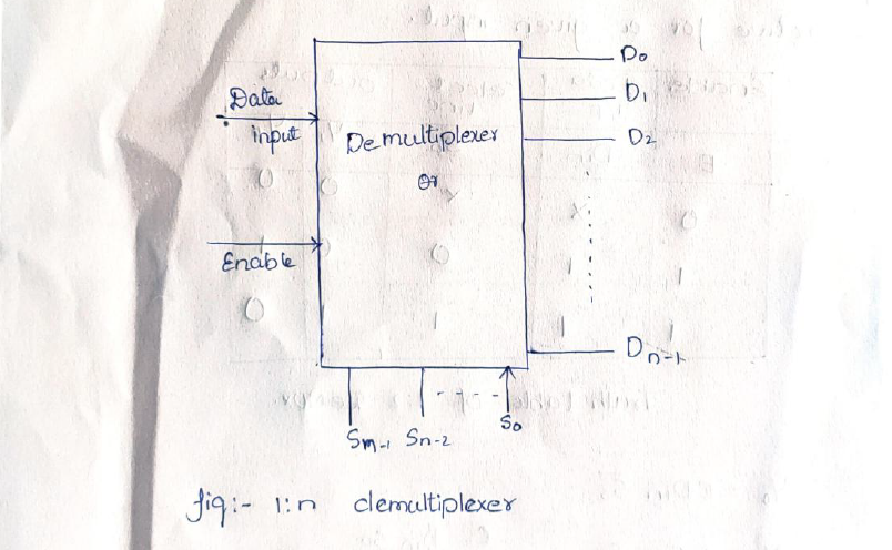
Types of Demultiplexers:
- 1-to-2 Demux: One input, two output lines, and one control line.
- 1-to-4 Demux: One input, four output lines, and two control lines.
- 1-to-8 Demux: One input, eight output lines, and three control lines.
- Higher-order Demux: Similar principle but with more outputs and control lines.
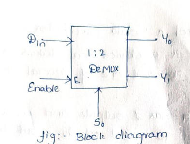
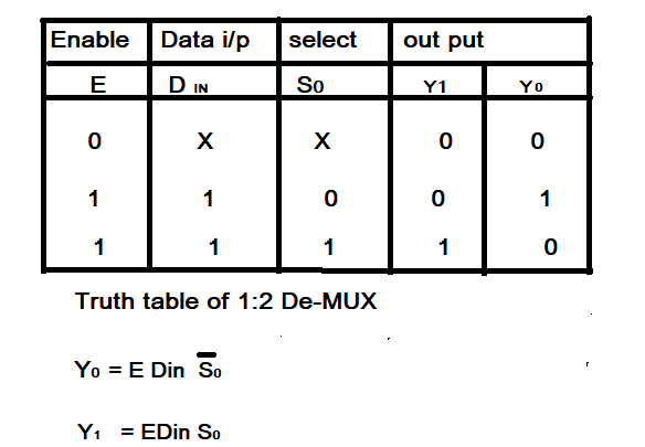
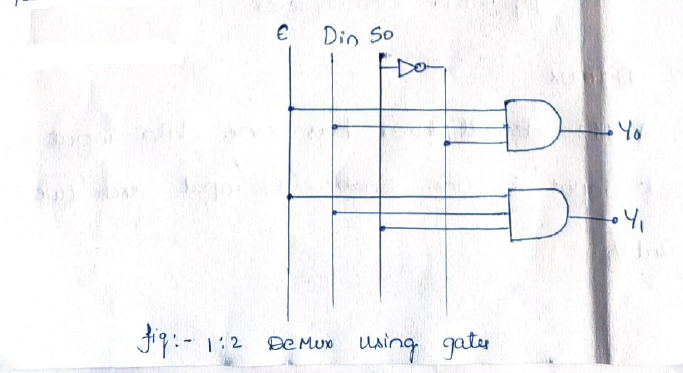
1 to 2 De-Mux
A 1-to-2 demultiplexer is a digital circuit that takes a single data input (Din) and distributes it to one of the two outputs (Y0 or Y1) depending on the value of the select input (S0). It also has an enable input (E), which controls the overall operation of the circuit.
The function block diagram, truth table, and logic diagram implementation is shown below.
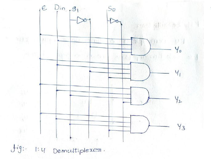
1×4 Demultiplexer (DEMUX)
A 1×4 Demultiplexer (DEMUX) is a digital circuit that takes 1 input data line and sends it to one of the 4 output lines based on 2 selection lines (control inputs). It is used to route data from a single source to multiple destinations.

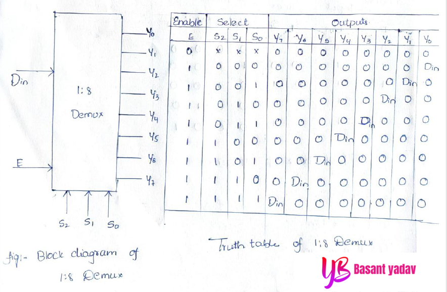
1×8 De-Multiplexer:
A 1×8 De-Multiplexer (DEMUX) is a digital circuit that takes one single input and distributes it to one of the eight outputs based on the combination of three selection lines (S2, S1, S0). It is also called a data distributor because it sends the input data to a specific output line while keeping the other outputs disabled.
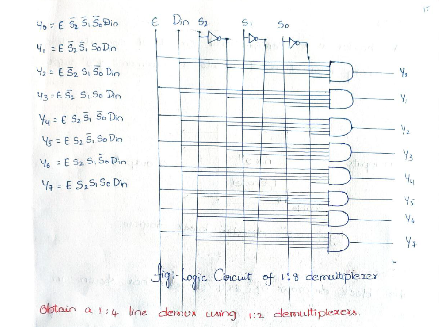
The logic diagram of implementation 1×8 De-MUX is shown
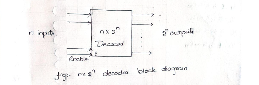
Decoder:
A decoder is a type of combinational circuit that converts n input binary codes into a maximum of 2ⁿ unique outputs. It is purely combinational, meaning its outputs depend only on the present inputs (not on any previous values, so no memory is involved.
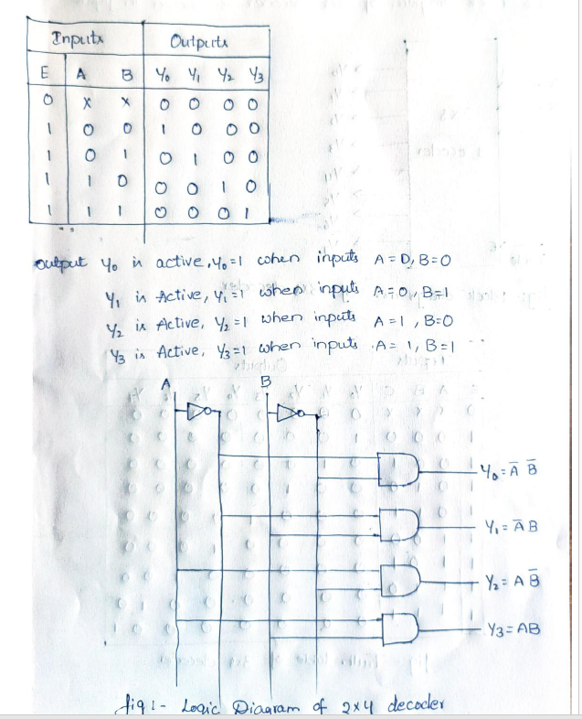
2 to 4 Decoder
A 2 to 4 Decoder is a combinational logic circuit that takes 2 binary inputs and generates 4 unique outputs. For every possible combination of the two inputs, exactly one output becomes active (logic 1) while all others remain inactive (logic 0).
It is implemented using AND gates and NOT gates, where each output represents a minterm of the input variables.

3 to 8 Decoder
A 3-to-8 Decoder is a combinational logic circuit that has 3 input lines and 8 output lines. For each possible input combination, only one output becomes active (logic 1), and all the others remain inactive (logic 0).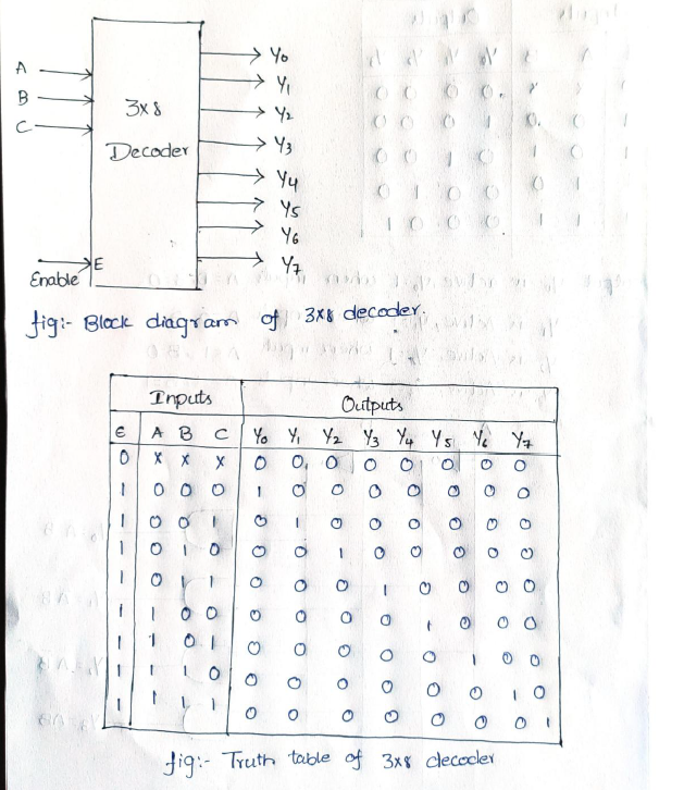
The logic diagram implementation and the Boolean expression of 3 to 8 decoder are shown below.

Encoder:
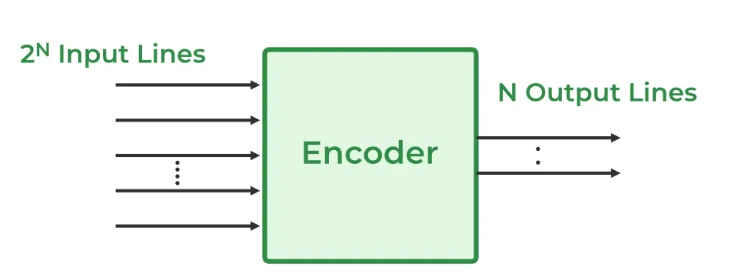
An Encoder is a combinational logic circuit that performs the reverse operation of a Decoder. While a decoder converts binary inputs into a single active output, an encoder converts multiple input signals into a coded binary output. In simple terms, an encoder takes 2^n input lines and encodes them into n output lines.
The functional block diagram of the encoder is shown in diagram
Types of Encoders
- 4 to 2 Encoder
- 8 to 3 Encoder (Octal Encoder)
- Decimal to BCD Encoder
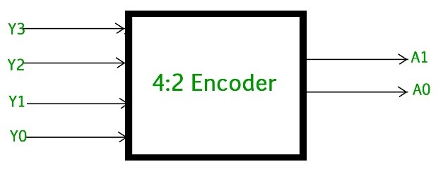
4 to 2 encoder
A 4 to 2 encoder is an encoder that has 4 input lines and 2 output lines. It converts the active input into a 2-bit output code. The output depends on which one of the four input lines is active.The block diagram of a 4 to 2 encoder is shown in the figure below.
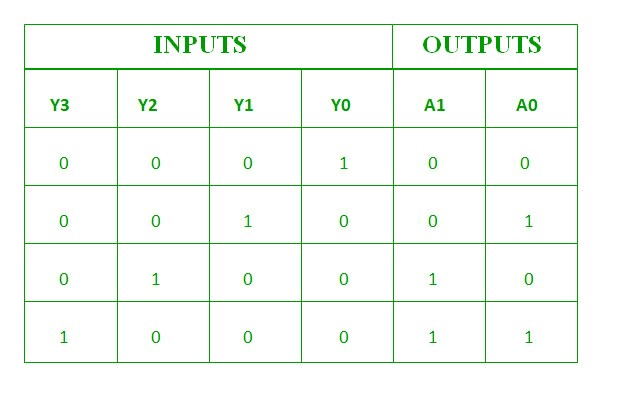
The Boolean expression for A1 and A0:
A1 = Y3 + Y2…………….1)
A0 = Y3 + Y1…………..2)
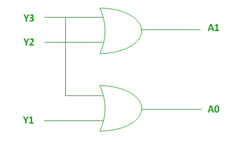
Logic Diagram implementation
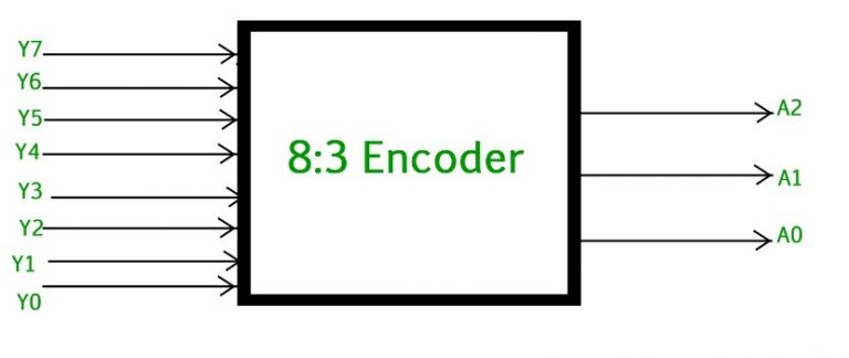
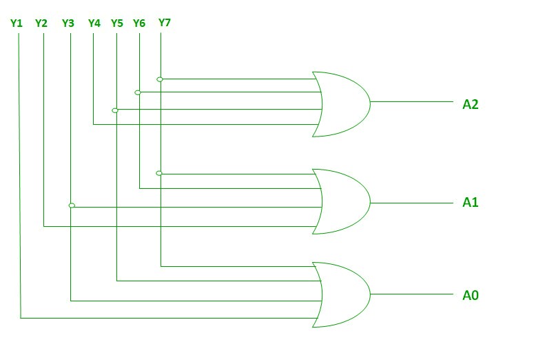
8 to 3 Line Encoder
An 8 to 3 line encoder is a combinational digital circuit that converts information from eight input lines into a three-bit binary code. Since 8 equals 2³, the encoder uses three output bits to identify which input line is active. The functional block diagram of 8 to 3 encoder is shown in the diagram.
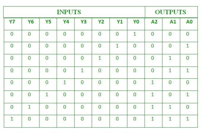
Boolean expression for A2, A1 and A0:
A2 = Y7 + Y6 + Y5 + Y4
A1 = Y7 + Y6 + Y3 + Y2
A0 = Y7 + Y5 + Y3 + Y1
The logic diagram of the implementation of 8 to 3 encoder is shown in the diagram
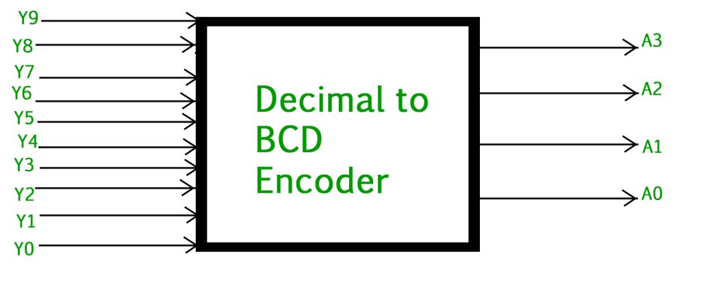
3. Decimal to BCD Encoder
The decimal-to-binary encoder has 10 input lines and 4 output lines. Each input represents a decimal number from 0 to 9, and the four output lines give the BCD (Binary Coded Decimal) form of that number. This encoder takes a decimal input and converts it into its BCD code, which appears at the output. The figure below shows the functional block diagram of a decimal-to-BCD encoder.