
Semiconductors
A semiconductor is a material that can conduct electricity, but not as well as a conductor. It conducts electricity better than an insulator. For example, copper is a conductor, and rubber is an insulator. Silicon and germanium are common semiconductor materials. The electrical conductivity of a semiconductor can change when the temperature, light, or impurities change.
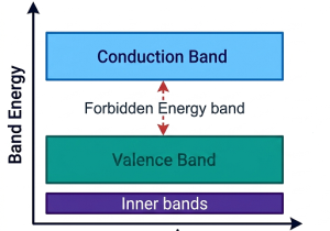
Semiconductors are very important because they are used in almost all electronic devices. Each semiconductor atom has four valence electrons. It also has a small energy gap between the valence band and the conduction band. At 0 K (absolute zero temperature), a semiconductor acts like an insulator because there are no free electrons to carry electricity.
Properties of Semiconductors
- Semiconductors conduct electricity better than insulators but not as well as conductors.
- Their resistance is higher than that of conductors and lower than that of insulators.
- As the temperature increases, the conductivity of a semiconductor increases.
- The resistance of a semiconductor decreases when the temperature increases.
- Adding impurities (doping) changes the electrical conductivity of a semiconductor.
- Semiconductors have a small energy gap (about 0.1 eV to 2.5 eV) between the valence band and the conduction band.
- Semiconductor atoms, such as silicon and germanium, have four valence electrons.
- At absolute zero temperature (0 K), a semiconductor behaves like an insulator.
- Semiconductors are widely used to make diodes, transistors, integrated circuits (ICs), LEDs, and many other electronic devices.
Bonds in Semiconductors and Their Crystal Structure
Semiconductor materials such as silicon (Si) and germanium (Ge) have four valence electrons in their outermost shell. To become stable, each atom shares its four valence electrons with four neighboring atoms. This sharing of electrons forms a covalent bond.
A covalent bond is a bond formed when two atoms share one or more pairs of electrons. These bonds hold the atoms together and make the semiconductor crystal strong and stable.
The atoms in a semiconductor are arranged in a regular and repeating pattern called a crystal structure. In this structure, each silicon or germanium atom is surrounded by four neighboring atoms. Every atom is connected to its neighbors by four covalent bonds.
At 0 K (absolute zero temperature), all the covalent bonds are complete, so there are no free electrons. Therefore, the semiconductor behaves like an insulator.
When the temperature increases, some covalent bonds break. This releases free electrons, leaving behind holes. The free electrons and holes help in the flow of electric current. As a result, the electrical conductivity of the semiconductor increases.
Silicon (Si) as a Semiconductor Material
Silicon (Si) is the most widely used semiconductor material in the electronics industry. It is found naturally in sand and quartz and is easy to obtain. Silicon has four valence electrons, which allow it to form four covalent bonds with neighboring atoms. These bonds create a strong and stable crystal structure.
At room temperature, silicon has moderate electrical conductivity. At 0 K (absolute zero), it behaves like an insulator because there are no free electrons. When the temperature increases, some electrons gain energy and move to the conduction band. These free electrons and the holes left behind help electric current flow.
Silicon is preferred over germanium because it can work at higher temperatures, is more stable, less expensive, and is available in large quantities. It is also easy to make into electronic devices.
Characteristics of Silicon
- Silicon is a semiconductor that conducts electricity better than an insulator but not as well as a conductor.
- Its chemical symbol is Si.
- Its atomic number is 14.
- It has four valence electrons, which help it form covalent bonds.
- It forms a strong crystal structure by sharing electrons with four neighboring silicon atoms.
- It is hard, brittle, and gray in color.
- It is the second most abundant element in the Earth’s crust, after oxygen.
- It can work at high temperatures, making it suitable for electronic devices.
- Its electrical conductivity increases when the temperature increases.
- Its conductivity can be controlled by adding impurities (doping).
- It is less expensive and more widely available than germanium.
- It has a small energy gap of about 1.1 eV at room temperature.
- It is chemically stable and has a long operating life.
- It is widely used in electronic devices, such as diodes, transistors, integrated circuits (ICs), solar cells, and microprocessors.
Germanium (Ge) as a Semiconductor Material
Germanium (Ge) is one of the first semiconductor materials used in electronic devices. It is a semiconductor because it conducts electricity better than an insulator but not as well as a conductor.
Germanium has four valence electrons. It shares these electrons with four nearby germanium atoms to form covalent bonds. This creates a strong and stable crystal structure.
At 0 K (absolute zero), germanium acts like an insulator because there are no free electrons. When the temperature increases, some electrons gain energy and move to the conduction band. These free electrons help electricity flow.
Germanium has higher conductivity than silicon at room temperature, but it cannot work well at high temperatures. Today, silicon is used more often because it is cheaper, more stable, and can work at higher temperatures.
Characteristics of an Insulator
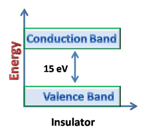
- The forbidden energy gap (Eg) is very large.
- Valence band electrons are tightly bound to their atoms and cannot move freely.
- The value of the forbidden energy gap for an insulator is approximately 10 eV.
- Due to the large band gap, electrons cannot easily jump from the valence band to the conduction band at room temperature.
- Some insulators may show a small amount of conduction when the temperature increases because a few electrons gain enough energy to cross the band gap.
- The electrical resistivity of an insulator is of the order of 107 Ω⋅m10^7\ \Omega\cdot\text{m} or higher.
- Therefore, insulators do not conduct electricity under normal conditions.
Examples: Glass, rubber, plastic, porcelain, mica, wood, and diamond.
Energy band diagram of semiconductor
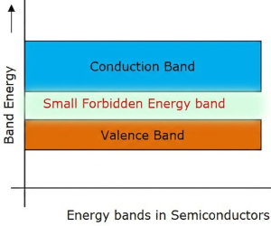
Semiconductors are such materials in which the forbidden energy gap is small and the conduction takes place if some external energy is applied. Examples: Silicon, Germanium. The following figure shows the structure of energy bands in semiconductors.
Characteristics of Semiconductors
The following are the main characteristics of semiconductors:
- The forbidden energy gap (Eg) is small, allowing electrons to move to the conduction band with a small amount of energy.
- The energy band gap is approximately 0.7 eV for Germanium (Ge) and 1.1 eV for Silicon (Si).
- A semiconductor is neither a good conductor nor a good insulator. Its electrical conductivity lies between that of a conductor and an insulator.
- As the temperature increases, more electrons gain enough energy to cross the band gap, so the conductivity of a semiconductor increases.
- The electrical conductivity of a semiconductor is of the order of 10210^2 mho/m (S/m).
- Semiconductors are widely used in the manufacture of diodes, transistors, integrated circuits (ICs), and other electronic devices.
Energy band diagram of a conductor
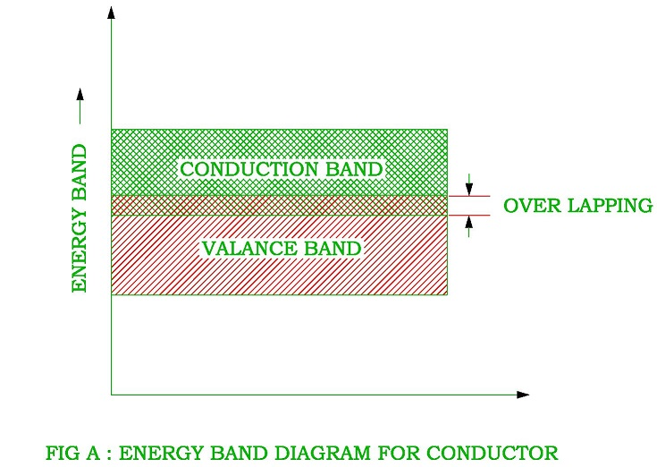
In a conductor (metal), the valence band (VB) and the conduction band (CB) overlap. Because there is no forbidden energy gap (band gap) between them, electrons can move freely from the valence band to the conduction band.
Hole Current
Hole current is the flow of holes (positive charge carriers) in a semiconductor. A hole is created when an electron leaves its position in the atomic lattice, leaving behind an empty space called a hole. As electrons move from one atom to another, the holes appear to move in the opposite direction.
Electron Current
Electron current is the flow of free electrons (negative charge carriers) through a semiconductor. It is one of the main types of current responsible for electrical conduction in semiconductor materials.
Difference Between Hole Current and Electron Current
| Hole Current | Electron Current |
|---|---|
| Caused by the movement of holes. | Caused by the movement of free electrons. |
| Holes behave as positive charge carriers. | Electrons are negative charge carriers. |
| Holes move opposite to the movement of electrons. | Electrons move from the negative terminal to the positive terminal. |
| Dominant in p-type semiconductors. | Dominant in n-type semiconductors. |
| Depends on doping, temperature, electric field, and material properties. | Depends on doping, temperature, electric field, and material properties. |
Types of Semiconductors
Semiconductors are classified into two main types based on their purity and the presence of impurities
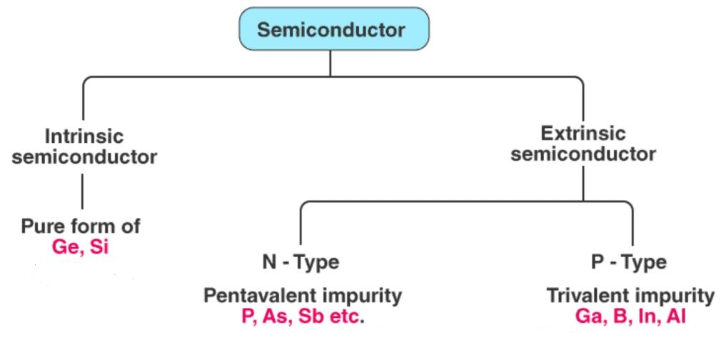
1. Intrinsic Semiconductor : An intrinsic semiconductor is a pure semiconductor that contains no intentionally added impurities. In an intrinsic semiconductor, the number of free electrons is equal to the number of holes. Examples: pure silicon and germanium
Characteristics of Intrinsic Semiconductor
- Made from pure silicon (Si) or germanium (Ge).
- No impurities are added.
- Equal number of electrons and holes.
- Low electrical conductivity at room temperature.
- Conductivity increases with temperature.
- Current is carried by both electrons and holes.
2. Extrinsic Semiconductor:An extrinsic semiconductor is a semiconductor whose electrical conductivity is increased by adding a small amount of impurities. This process is called doping.
Characteristics of Extrinsic Semiconductor
- Contains added impurities.
- Higher conductivity than an intrinsic semiconductor.
- More charge carriers are available.
- Widely used in electronic devices.
- Divided into n-type and p-type semiconductors.
A. n-Type Semiconductor:
An n-type semiconductor is formed by doping pure silicon or germanium with a pentavalent impurity (an atom with five valence electrons), such as phosphorus (P), arsenic (As), or antimony (Sb).
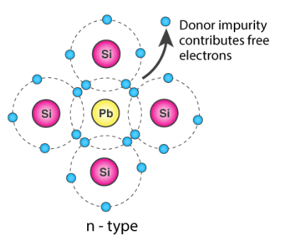
Characteristics of an n-Type Semiconductor:
- An n-type semiconductor has Majority charge carriers are electrons.
- An n-type semiconductor has Minority charge carriers are holes.
- An n-type semiconductor contains many free electrons.
- An n-type semiconductor conducts electricity mainly through electrons.
- An n-type semiconductor has Higher conductivity than an intrinsic semiconductor
B. p-Type Semiconductor
A p-type semiconductor is formed by doping pure silicon or germanium with a trivalent impurity (an atom with three valence electrons), such as boron (B), aluminium (Al), gallium (Ga), or indium (In).
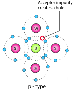
Characteristics p-Type Semiconductor
- p-Type Semiconductor has majority charge carriers that are holes.
- p-Type Semiconductor has Minority charge carriers that are electrons.
- -Type Semiconductor contains many holes.
- -Type Semiconductor conducts electricity mainly through holes.
- -Type Semiconductor has Higher conductivity than an intrinsic semiconductor.
Difference Between Intrinsic and Extrinsic Semiconductors
| Intrinsic Semiconductor | Extrinsic Semiconductor |
|---|---|
| Pure semiconductor | Semiconductor with added impurities |
| No doping | Doping is required |
| Equal number of electrons and holes | Unequal number of electrons and holes |
| Lower electrical conductivity | Higher electrical conductivity |
| Examples: Pure silicon, pure germanium | Examples: n-type and p-type semiconductors |
Comparison Between n-Type and p-Type Semiconductors
| n-Type Semiconductor | p-Type Semiconductor |
|---|---|
| Formed by doping a pure semiconductor with pentavalent (5-valence-electron) impurities. | Formed by doping a pure semiconductor with trivalent (3-valence-electron) impurities. |
| Majority charge carriers are electrons. | Majority charge carriers are holes. |
| Minority charge carriers are holes. | Minority charge carriers are electrons. |
| Conducts electricity mainly through electrons. | Conducts electricity mainly through holes. |
| Contains a large number of free electrons. | Contains a large number of holes. |
| Donor impurities provide extra electrons. | Acceptor impurities create holes by accepting electrons. |
| The Fermi level lies closer to the conduction band. | The Fermi level lies closer to the valence band. |
| Common dopants are Phosphorus (P), Arsenic (As), and Antimony (Sb). | Common dopants are Boron (B), Aluminium (Al), Gallium (Ga), and Indium (In). |
| The semiconductor remains electrically neutral overall. | The semiconductor remains electrically neutral overall. |
| Used in n-type regions of diodes, transistors, integrated circuits (ICs), and other electronic devices. | Used in p-type regions of diodes, transistors, integrated circuits (ICs), and other electronic devices. |
Charge Carriers:
A charge carrier is a particle that carries electric charge and allows electric current to flow through a semiconductor. In semiconductors, the two types of charge carriers are electrons and holes. There are two types of charge carriers: the are Majaority charge carrier and the minority charge carrier.
Majority Charge Carrier
A majority charge carrier is the type of charge carrier that is present in the largest number in a semiconductor and carries most of the electric current. In a p-type semiconductor, the majority charge carrier is a hole, and the majority charge carrier is an electron.
Minority Charge Carrier
A minority charge carrier is the type of charge carrier that is present in a smaller number in a semiconductor. In an n-type semiconductor, holes are the minority charge carriers, and in a p-type semiconductor, electrons are the minority charge carriers.
Effect of Temperature on Conductivity:
The conductivity of a semiconductor changes with temperature. When temperature increases, the number of charge carriers also increases, so the conductivity of semiconductor increases.
1. At Low Temperature:
- At very low temperature (near absolute zero), very few electrons get energy.
- Only a few electrons are excited from valence band to conduction band.
- So, number of charge carriers is very small.
- Therefore, conductivity is very low.
2. At Normal Temperature:
- At room temperature, more electrons get energy.
- More electrons move from valence band to conduction band.
- Number of electrons and holes increases.
- So, conductivity increases.
3. At High Temperature:
- When temperature is high, a large number of electrons get energy.
- Many electrons jump to conduction band.
- Number of free electrons and holes increases rapidly.
- Therefore, conductivity increases very fast.
Compiled by Er. Basant Kumar Yadav