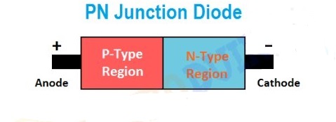
A P-N junction is an interface or a boundary or contact surface between two P-type and N-type semiconductor material. Actually, P-N junction is made by doping trivalent and pentavalent impurities on a piece of pure semiconductor and heating it to high temperature.
P-N Junction diode or Semiconductor Diode:
A p-n junction diode is a two-terminal device that conducts current only in one direction. A symbol of P-N junction diode is shown in figure (ii). Triangular side represents the p-type and vertical bar represent n-type semiconductor. The arrow in the symbol indicates the direction of flow of current when it is in forward biased condition.
(Fig (i): P-N junction diode)(Fig (ii): symbol of P-N junction diode)
Depletion layer and Barrier Potential in a P-N Junction Diode
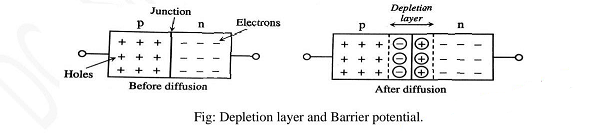
As soon as p-n junction is formed, the charge carriers diffuse from a region of high concentration to a region of low concentration. So, the electrons from the n-region diffuse into the p-region when they combine with the holes and get neutralized. Similarly, the holes from the p-region diffuse into the N-region and combine with electrons to get neutralized.
The p-region near the junction is left with immobile negative ions and n-region near the junction with immobile positive ions due to the electron hole recombination. So, a thin layer around the junction becomes depleted of free charge carrier. This region is called depletion region. Its thickness is of the order of a few microns. The width of depletion layer decreases in forward biased condition and increases in reverse biased condition of p-n junction diode.
Due to migration of electrons and holes from two regions and their recombination, the n-region gains excess positive charge and p-region the excess negative charge. These charges near the junction establish an electric field across the junction directed from the n-region to the p-region. This field produces a potential difference which prevents further diffusion of the electrons from n-region to p-region. This p.d is called barrier potential, VB. The barrier potential is about 0.3V for germanium and 0.7V for silicon at the room temperature. The barrier potential depends on doping density, electronic charge and temperature. When temperature increases the barrier potential decreases and vice versa for a given p-n junction diode.
Biasing of P-N Junction Diode:
Biasing is the process of applying an external electric field by connecting the diode to an external battery to produce and maintain the flow of charge carriers through the p-n junction. The junction diode can be biased in the following two ways.
a) Forward Biasing
A diode is said to be forward biased if its P-type is connected to positive terminal and N-type to negative terminal of battery as shown in figure below. During forward biasing, majority charge carriers in P and N type semiconductor are pushed towards the junction and crossed the barrier and minority charge carriers are pulled away from the junction. As a result, large current appears in the circuit due to the majority charge carriers. In forward biased condition,
(i) Width of depletion layer slowly decreases and finally vanish. (ii) Potential barrier decreases [V–V₍ᴮ₎] and finally becomes zero. (iii) Flow of current inside diode is due to majority charge carrier. (iv) Diode offers very low resistance called forward bias resistance. (v) The diode acts as a closed switch.
(vi) Total current is the sum of electron diffusion current and hole diffusion current.
b) Reverse Biasing
A diode is said to be reverse biased if its P-type is connected to negative terminal and N-type to positive terminal of battery. During reverse biasing, majority charge carriers cannot cross the junction but minority charge carriers in P and N type semiconductor are pushed towards the junction and crossed the barrier. As a result, small current in reverse direction appears in the circuit due to the minority charge carriers. In reverse biased condition,
When diode if reverse biased, i. Width of depletion layer increases, ii. Potential barrier is increased [V + V₍ᴮ₎] iii. Flow of small current inside diode is due to minority charge carrier. iv. Diode offers very high resistance called reverse bias resistance. v. The diode acts as open switch.
Characteristics of P-N Junction Diode:
The graphical relationship between current and potential difference across the junction diode is called characteristics of the diode. It is also known as I-V characteristics of the junction diode.
a) Forward Bias Characteristics It is the graphical relationship between forward current and forward voltage. The circuit diagram for studying forward characteristics of P-N junction diode is shown in figure.
The voltmeter (V) measures the potential difference across the diode and milliammeter (mA) measures the current flows through it. The forward voltage across the diode is varied with the help of rheostat and corresponding diode current is noted. A graph of current versus voltage is plotted which is show in graph. This graph represents the forward characteristics of the p-n junction diode.
From the graph it is seen that,
The current remains zero until forward voltage is small.
As forward voltage is further increased, the current begins to flow in the diode. The forward current increases slowly up to certain forward voltage called the knee voltage or threshold voltage. It is numerically equals to the barrier potential.
After knee voltage, current increases rapidly and the curve is almost linear. Knee voltage is about 0.3 V for germanium and 0.7V for silicon.
b) Reverse Bias Characteristics
It is the graphical relation between reverse current and reverse voltage. The circuit diagram for studying reverse characteristics is shown in figure below.
The voltmeter measures the reverse voltage and microammeter measures the reverse current flows through the diode. The reverse voltage across the diode is varied with the help of rheostat and the corresponding reverse current is noted by microammeter.
A graph of reverse current versus reverse voltage is shown in figure. This graph represents the reverse characteristics of the diode.
When the diode is reverse biased, it is seen that,
When the reverse voltage is increased from zero, the reverse current also increases slightly over a long range.
When the reverse voltage is increased beyond a certain value called the breakdown voltage, the reverse current suddenly and sharply increases and the junction is said to have been breakdown.
The majority charge carriers are blocked and only a small current flow through the diode due to minority charge carriers.
The reverse voltage at which the diode current starts to increase sharply is called break down voltage. The break down voltage depends on the density of doping and the thickness of depletion region.
Application of Diode a) Used as a rectifier in power supply system. b) It is also used in signal processing system. c) Used in logical circuit system. d) A switch in logic circuits used in computers.
Rectification
Rectification is the process in which ac in converted into dc. The device which is used for rectification is called a rectifier. When p-n junction diode is forward biased, it offers low resistance and current flows through it. But when reverse biased, it offers high resistance and no current flows through it. This unidirectional property of a junction diode enables to be used as a rectifier.
There are two types of rectifiers:
a) Half wave rectifier b) Full wave rectifier(There are two types of full wave bridge rectifier) a. Center Tapped Full Wave Rectifier b. Bridge Rectifier
Full Wave Rectifier:
The circuit that converts complete cycle of input alternating signal or current into direct signal or current called full wave rectifier. One of full wave rectifier is center tapped full wave rectifier.
Center Tapped Full Wave Rectifier:
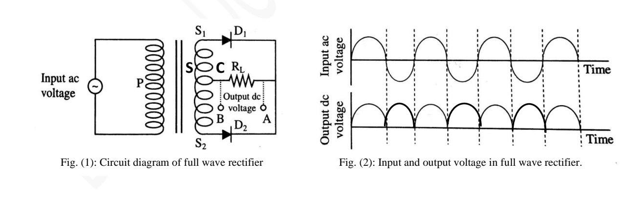
The circuit diagram of center tapped full wave rectifier consists of two diodes (D₁ and D₂) connected across secondary coil through load resistance (Rₗ) are connected as illustrated in fig. (1). In this connection, secondary coil is center tapped at ‘C’ and it is connected one terminals of each diode through load Rₗ.
When input voltage (Vin) is applied to across primary coil P, one terminal of secondary coil becomes most positive and another terminal becomes most negative during positive half cycle of input. Let ‘S1’ becomes most positive, ‘S2’ becomes negative and center tapped point ‘C’ becomes intermediate between them. This makes diode D1 forward based and diode D2 becomes reverse biased. Thus, current flows through circuit and load RL due to only D1.
During another half cycle of input, polarity of terminals changes, terminal ‘S1’ becomes most negative and terminal ‘S2’ becomes most positive converting D1 into forward biased and D2 into reversed biased condition. Thus, current flow flows through RL due to only D2.
This converts a complete cycle of input ac signal into dc. This process is repeated continuously for other cycles of input converting all entire ac signals into dc and hence circuit acts as half wave rectifier. This gives output as shown in the graph.
Full wave Bridge Rectifier
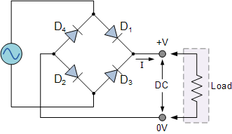
A full-wave bridge rectifier is an electronic circuit that converts an alternating current (AC) into a pulsating direct current (DC). It uses a bridge configuration of four diodes to rectify both the positive and negative halves of the AC waveform, resulting in a more efficient and smoother DC output than a half-wave rectifier.
Working Mechanism of Full Wave Bridge Rectifier:
The circuit consists of four diodes (D1, D2, D3, and D4 and a load resistor (RL), typically arranged in a diamond shape.
The circuit consists of four diodes (D1, D2, D3, and D4) arranged in a bridge configuration and a load resistor RL. During the positive half-cycle of the input AC voltage, diodes D1 and D2 conduct, allowing current to flow through RL in one direction. During the negative half-cycle, diodes D3 and D4 conduct, again directing current through RL in the same direction. This results in full-wave rectification without requiring a center-tapped transformer.
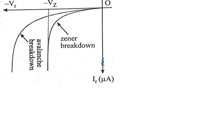
Reverse Breakdown
Reverse biasing voltage at which reverse current rises abruptly is called reverse breakdown voltage. At this voltage, crystal structure breaks down and maximum current flows by increasing reverse bias voltage.
1. Zener Breakdown: Depletion region is very narrow in heavily doped junction diode. It set up the strong potential gradient in depletion layer that is able to pull out electrons in addition of small reverse bias potential. Reverse diode current increases very sharply. This is because, when reverse bias voltage is applied, electric field at the junction further increases and pulls out electrons from the valence band creating electron hole pairs. This is called Zener effect or Zener breakdown.
NOTE: Higher is the doping level, more will be the concentration of impurity in diode, thinner will be the width of depletion layer, larger will be the potential gradient in depletion layer, and hence will easy to pull out electrons from covalent bond in addition of reverse biasing voltage. This causes to decrease in Zener breakdown voltage with increase in doping level.
2. Avalanche Breakdown: Depletion region is a bit wider in weakly doped junction diode than heavily doped junction diode. It set up weak potential gradient in depletion layer that is not able to pull out electron from covalent bond.
Reverse diode current increases gradually. This is because, when reverse voltage is applied, minority charge carriers are accelerated in this region and ionize atoms by collision producing electrons. These electrons further ionize to other atoms getting accelerated. This produces avalanche of flow of electrons in diode and flow of large current. This is called avalanche effect or avalanche breakdown.
Zener Diode:
A heavily doped diode that has a sharp breakdown voltage is called Zener Diode. The depletion layer of Zener Diode is very thin. It is operated under reverse bias condition. It is specially used as a voltage regulator. The circuit symbol of Zener Diode is as below.
(Fig: Symbol of Zener diode)
It is just like an ordinary diode except that the bar is turned into Z-shape.
Zener Diode Characteristics:
Zener diode has forward bias characteristics same as that of ordinary PN junction diode. But it has sharp breakdown voltage in reverse bias. When forward biasing voltage increases from zero, forward current increases very slowly. But after reaching
particular potential, it increases rapidly. At this voltage, forward biasing voltage makes to disappear depletion layer and hence disappear barrier potential. With potential above knee voltage, diode offers very small or almost negligible resistance.
When reverse biasing voltage (magnitude of negative potential) increases from zero, reverse bias current is almost zero. But, after reaching particular potential it increases sharply. This voltage is Zener breakdown voltage.
Difference between Ordinary PN Junction diode and Zener diode:
Ordinary Diode
Zener Diode
In ordinary diode, diode is commonly doped.
In Zener Diode, diode is heavily doped.
It works on forward bias.
It works on reverse bias.
Depletion layer is wider and potential gradient is less in depletion layer.
Depletion layer is narrower than ordinary diode and potential gradient is larger in depletion layer.