
A transistor is a three-terminal semiconductor device used to amplify or switch electronic signals and electrical power. It is the basic building block of modern electronics.
Types of transistor
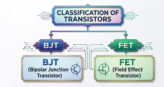
Introduction of Bipolar Junction Transistor (BJT)
A Bipolar Junction Transistor (BJT) is a three-terminal semiconductor device made up of two PN junctions. It is mainly used to amplify electrical signals and can also be used as an electronic switch. A BJT has three terminals: Base, Collector, anf Emitter.
1.NPN Transistor:
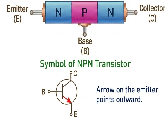
Emitter
It is one of the terminals of the BJT which supplies charge carriers (i.e. electrons in NPN transistor and holes in a PNP transistor) to the base region. It is an outer region situated in one side of transistor. This region is the most highly doped region.
Base
The base is the middle part of a transistor. It controls the flow of charge carriers from the emitter to the collector. The base is very thin and lightly doped, so most of the charge carriers can pass through it easily. It is placed between the emitter and collector and is the smallest region of a transistor.
Collector
The collector is one of the three regions of a transistor. Its main function is to collect charge carriers from the base and emitter so that current can flow through the transistor. The collector is moderately doped and is larger than the emitter. Its larger size helps it handle high current and remove the heat produced during the operation of the transistor
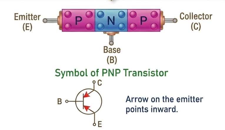
2 PNP TRANSISTOR
A PNP transistor is made of two P-type semiconductor materials separated by a thin layer of N-type material. In other words, the N-type material is placed between two P-type materials. The two P-type regions work as the emitter and collector, while the N-type region works as the base. Holes are the majority charge carriers in a PNP transistor. The arrow on the emitter points from the P-region toward the N-region. Therefore, the conventional current flows from the emitter to the base. The symbol of a PNP transistor is shown in Figure
There are two types of transistors: NPN and PNP. Among them, the NPN transistor is more widely used. In an NPN transistor, current conduction mainly occurs due to electrons, while in a PNP transistor, it mainly occurs due to holes. Since electrons can move faster than holes, an NPN transistor generally has higher current conduction than a PNP transistor.
Working Principle of NPN Transistors
An NPN transistor consists of two N-type semiconductor regions (Emitter and Collector) and one P-type semiconductor region (Base).
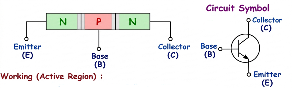
Working Principle (Active Region)
- The base-emitter (B-E) junction is forward biased, while the base-collector (B-C) junction is reverse biased.
- In an NPN transistor, electrons are the majority charge carriers.
- When the B-E junction is forward biased, electrons are emitted from the N-type emitter into the P-type base.
- The base is very thin and lightly doped, so only a small number of electrons recombine with holes in the base.
- Most of the electrons pass through the base and are attracted toward the N-type collector because the B-C junction is reverse biased.
- Therefore, a small base current (I_B) controls a large collector current (I_C).
Circuit for NPN Transistor in Active Region
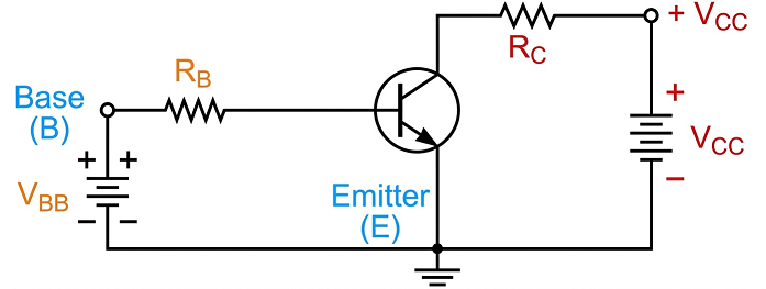
So, in NPN transistor IE = IC + IB and IC >>IB (A small input at base controls a large output between collector and emitter.)
Working Principle of PNP Transistors
A PNP transistor consists of two P-type semiconductor regions (Emitter and Collector) and one N-type semiconductor region (Base).
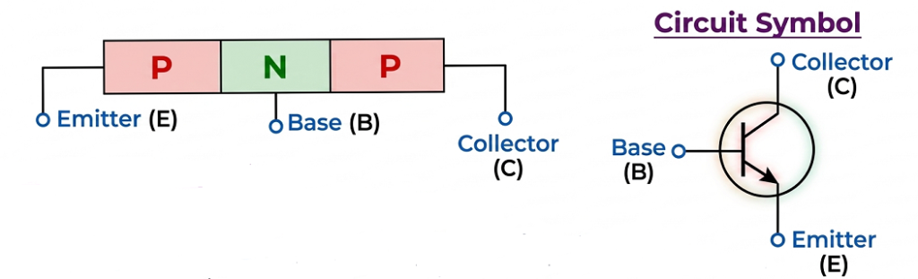
Working Principle (Active Region)
- The base-emitter (B-E) junction is forward biased, while the base-collector (B-C) junction is reverse biased.
- In a PNP transistor, holes are the majority charge carriers.
- When the B-E junction is forward biased, holes are emitted from the P-type emitter into the N-type base.
- The base is very thin and lightly doped, so only a small number of holes recombine with electrons in the base.
- Most of the holes pass through the base and are attracted toward the P-type collector because the B-C junction is reverse biased.
- Therefore, a small base current (I_B) controls a large collector current (I_C).
Circuit for PNP Transistor in Active Region
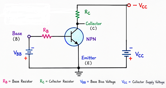
So, in NPN transistor IE = IC + IB and IC >>IB (A small input at base controls a large output between collector and emitter.)
CONFIGURATIONS OF BJT
A BJT (Bipolar Junction Transistor) has three terminals: Emitter (E), Base (B), and Collector (C). By choosing a different terminal as common to both input and output circuits, we get three basic configurations of BJT.
The three configurations are:
- Common Base (CB) Configuration
- Common Emitter (CE) Configuration
- Common Collector (CC) Configuration
1.Common Base (CB) Configuration:
In common base configuration, the base terminal is common to both the input and output circuits. The input is applied between emitter and base and the output is taken between collector and base.The circuit diagram of common base configuration is shown in diagram.
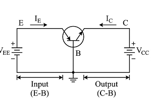
In a Common Base (CB) configuration, the current gain is denoted by the Greek letter α (alpha) and is defined as the ratio of the output collector current IC to the input emitter current IE. And given by